Table of Contents
The NITI Frontier Tech Hub (under NITI Aayog), in a report compiled with KPMG titled “Future of India’s Semiconductor Industry,” has unveiled a comprehensive 10-year roadmap. Released by the Ministers of Finance and IT, the report charts India’s path from its nascent position to building a $120–150 billion semiconductor value chain by 2035.
Key Highlights of the Report
- Vision 2047: The roadmap emphasizes that domestic semiconductor capability is “imperative to India’s aspiration to become a developed nation by 2047.” It urges India to shift gears from being a major consumer of chips to becoming an “indispensable part of the global semiconductor value chain.”
- Five Strategic Pillars: The strategy is anchored around five mutually reinforcing pillars:
- Pioneering: Focus on R&D, advanced design Intellectual Property (IP) creation (targeting over 100 advanced design IPs), and AI-native chip design.
- Policy and Investment: Ensuring policy stability and mobilizing long-term capital for deep-tech capabilities.
- Production: Shifting focus towards advanced packaging, Outsourced Semiconductor Assembly and Testing (OSAT), and wide-bandgap/compound semiconductors.
- People: Developing a national talent pyramid tailored to advanced design and manufacturing.
- Partnership: Forging global strategic tie-ups with trusted nations for critical minerals and supply chain integration.
- Synergy with ISM 2.0: The roadmap aligns directly with the India Semiconductor Mission (ISM) 2.0, marking a transition from mere “ecosystem creation” to “ecosystem deepening.”
Why India Needs to “Shift Gears”?
- High Import Dependence: The local ecosystem currently cannot meet domestic demand. Electronics assembled in India have an overwhelming share of imported components, leading to massive forex outflows (estimated at $150 billion between 2017 and 2025).
- National Security and Defence Risk: Deploying imported semiconductor components in sensitive aerospace and defence programs creates severe strategic and supply chain vulnerabilities.
- Powering Future Tech: Domestically manufactured chips will play a decisive role in making next-generation technologies—such as 5G/6G handsets, AI infrastructure, and electric mobility—affordable and secure.
Present Semiconductor Production Capacity of India (As of 2026)
India’s transition from a pure-play chip design hub to an active fabrication and packaging ecosystem has accelerated significantly under the India Semiconductor Mission (ISM), backed by an initial ₹76,000 crore fiscal incentive framework.
- The Scale of Approvals: As of mid-2026, India has approved 13 semiconductor projects (12 under ISM and 1 under the SPECS scheme) across six states, attracting total investment commitments exceeding ₹1.6 lakh crore.
- Commercial Operations: Commercial production has already commenced at two primary Outsource Semiconductor Assembly and Test (OSAT) / Assembly, Testing, Marking, and Packaging (ATMP) facilities (including Micron’s facility in Sanand, Gujarat), with two more mega-plants slated to begin production later this year.
- The “Front-End” Fab Milestone: In May 2026, Tata Electronics signed a historic strategic agreement with Dutch lithography giant ASML to supply advanced equipment for India’s first premier 300-mm front-end commercial wafer fabrication plant in Dholera, Gujarat.
- Policy Evolution (ISM 2.0): The Union Budget 2026–27 allocated an unprecedented ₹8,000 crore for the sector, alongside launching ISM 2.0, which broadens the fiscal focus to raw materials, equipment manufacturing, and indigenous Intellectual Property (IP) development.
Major Approved Projects at a Glance
| Facility / Enterprise | Location | Core Focus | Scale / Investment |
| Tata Electronics & PSMC | Dholera, Gujarat | Commercial Fab (28nm node compute/power chips) | ~₹91,000 Crore / 50,000 wafers per month |
| Tata Semiconductor (TSAT) | Jagiroad, Assam | Advanced Chip Packaging & Assembly | ~₹27,000 Crore / 48 million chips per day |
| Micron Technology | Sanand, Gujarat | ATMP / Packaging for DRAM & NAND | Over ₹22,000 Crore |
| CG Power & Renesas | Sanand, Gujarat | OSAT for Automotive & Industrial applications | ~₹7,600 Crore |
Why Domestic Manufacturing of Semiconductors is Essential?
In its May 2026 comprehensive roadmap, the NITI Aayog designated semiconductors as an absolute imperative for India’s target to become a developed nation (Viksit Bharat) by 2047.
- Strategic Autonomy & National Security: Modern defense assets (missile guidance, secure satellite communications, radar) rely heavily on advanced silicon. Relying entirely on imports leaves critical military supply chains vulnerable to foreign embargoes or geopolitical blackmails.
- Mitigating the Import Burden: India’s domestic electronics demand is exploding, driven by 5G/6G, EVs, and domestic smartphone production. Local fabrication is required to stem massive foreign exchange outflows caused by importing nearly all foundational components.
- Capturing the “China-Plus-One” Pivot: Global hardware giants are actively decoupling centralized supply chains away from East Asia due to cross-strait tensions. India acts as a geopolitically stable, trusted democratic node in the international supply framework.
- Economic Multiplier Effect: Establishing a silicon base stimulates an entire upstream chemical, gas, and machinery ecosystem, fostering thousands of high-skilled industrial jobs and a robust deep-tech startup culture.
Can India Produce High-Capacity yet Sophisticated Semiconductors?
India is currently highly capable of producing high-volume legacy and mature chips (28nm to 40nm nodes), but cannot yet fabricate bleeding-edge sophisticated nodes (sub-5nm chips used in high-end smartphones and AI GPUs).
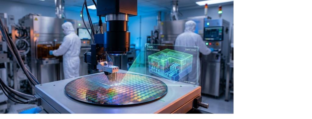
- Design Competency: India is already a global design superpower, housing roughly 20% of the world’s chip design workforce. Highlighting this, the government successfully taped out an indigenous 7nm processor design in late 2025.
- The Mature Node Strategy: Building high-capacity fabs at 28nm (like the upcoming Dholera facility) is a highly calculated, pragmatic choice. These are not “obsolete”—they are the heavy lifters for automotive, IoT, power modules, and consumer household electronics that drive the bulk of global consumer volume.
- The Bleeding-Edge Gap: Transitioning to ultra-sophisticated manufacturing requires hyper-stable infrastructure, complex chemical ecosystems, and billions of dollars in continuous capital expenditure. While India can scale up high-capacity output for mature nodes by 2027–2028, fabrication of state-of-the-art AI chips remains a medium-to-long-term milestone.
Key Challenges
- Infrastructure Vulnerabilities: Fabrication plants require non-negotiable 24/7 ultra-pure water systems and absolutely uninterrupted, fluctuation-free power grids. Minor power ripples can destroy an entire batch of multi-million dollar wafers.
- Underdeveloped Upstream Supply Chain: A chip fab requires thousands of ultra-high-purity chemicals, specialized gasses, and ultra-flat silicon ingots. India presently lacks localized chemical refinement that meets the strict parts-per-billion purity requirements of front-end fabs.
- Sustained Capital Intensity: Semiconductor manufacturing is notorious for rapid obsolescence cycles. Fabs require cyclical infusions of multi-billion dollar capital upgrades every few years, placing a severe fiscal strain on corporate balance sheets and state subsidy limits.
- The Talent Mismatch: While India boasts an abundance of software and chip architecture design talent, it faces a stark shortage of specialized process engineers, cleanroom operators, and materials scientists trained specifically in hardware fabrication.
Government Initiatives for Semiconductor Production in India
1. The Umbrella Framework: Semicon India Programme
Launched in December 2021 with a massive financial outlay of ₹76,000 crore, this flagship program provides uniform 50% fiscal support on a pari-passu basis for setting up semiconductor fabs, display fabs, compound semiconductors, and ATMP/OSAT facilities.
Evolution into India Semiconductor Mission (ISM) 2.0
The Union Budget 2026–27 formally launched ISM 2.0 to deepen domestic value addition, backed by a total financial outlay of ₹8,000 crore for the Modified Semiconductor Programme for FY 2026–27.
- Core Focus of ISM 2.0: Shifting attention toward localized production of semiconductor manufacturing equipment and raw materials, developing indigenous full-stack semiconductor Intellectual Property (IP), and creating industry-led R&D and training centers.
- Dedicated Allocation: A separate provision of ₹1,000 crore has been earmarked within the budget specifically to catalyze these ISM 2.0 long-term R&D pipelines.
2. Core Operational Schemes Under ISM
A. Scheme for Setting Up Semiconductor Fabs
- Objective: Attract mega-investments for building silicon CMOS-based wafer fabrication plants for logic, memory, analog, and digital Integrated Circuits (ICs).
- Incentive: 50% fiscal support on overall capital expenditure for both mature and advanced technology nodes.
- Key Progress: Enabled the establishment of India’s first flagship 300-mm commercial fab by Tata Electronics in Dholera, Gujarat.
B. Display Fabs Scheme
- Objective: Establish large-scale fabrication facilities for advanced display technologies like AMOLED and Thin-Film Transistor (TFT) LCDs.
- Incentive: Up to 50% financial support to de-risk high-capital asset creation in the display supply chain.
C. Modified Scheme for Compound Semiconductors and ATMP/OSAT
- Objective: Focuses on niche and specialty hardware fields, including Silicon Photonics, Sensors (MEMS), Gallium Nitride (GaN), and Silicon Carbide (SiC) foundries, alongside Assembly, Testing, Marking, and Packaging (ATMP) setups.
- Incentive: 50% capital expenditure subsidy. This has triggered high-capacity commercial rollouts, such as Micron’s memory packaging unit and Kaynes Semicon’s plant in Sanand, Gujarat.
D. Design Linked Incentive (DLI) Scheme
- Objective: Capitalize on India’s existing design strength (accounting for ~20% of the global chip design workforce) by supporting domestic MSMEs and startups.
- Financial Model: Backed by a ₹1,000 crore outlay, it offers product design infrastructure support (EDA tools, IP cores) and financial incentives up to ₹15 crore per company.
- Current Footprint: As of early 2026, the DLI scheme supports 24 active semiconductor design startups, which have successfully leveraged government backing to draw over ₹430 crore in private venture capital.
3. Supply Chain and Ancillary Schemes
Electronics Components Manufacturing Scheme (ECMS)
Recognizing that a semiconductor fab cannot operate in isolation, the government introduced the ECMS to capture the broader electronics component ecosystem.
- Originally rolled out with a focus on core components, the overwhelming response from global suppliers led the government to massively scale up its total outlay to ₹40,000 crore in the 2026–27 budget to maintain momentum.
Scheme for Promotion of Manufacturing of Electronic Components and Semiconductors (SPECS)
- Provides a 25% financial incentive on capital expenditure for targeted electronic components, sub-assemblies, and specialized semiconductor industrial sub-units.
4. Regulatory Reforms and Infrastructure Support
- Special Economic Zone (SEZ) Liberalization: The government overhauled SEZ Rules to ease land acquisition issues for deep-tech hardware setups. The minimum land requirement for electronics and semiconductor units was slashed from 50 hectares down to 10 hectares, and rules were modified to permit domestic market sales upon payment of basic duties.
- Dedicated Spatial Clusters: The central government officially notified specialized SEZs and fast-tracked industrial zoning with Inland Container Depot status for key corridors, such as the Tata Semiconductor zone in Dholera.
- Single-Window Investor Facilitation: In May 2026, the Ministry of Electronics and Information Technology (MeitY) launched a dedicated “Investors Support” Portal under the ISM to offer end-to-end regulatory clearances and statutory handholding for global ecosystem players.
5. Strategic International Alliances (Geopolitical Alignment)
To overcome immediate technology transfer deficits, India has integrated its domestic policy with bilateral technological corridors:
- The US-India iCET Framework: Drives collaborative research and safe public-private supply loops.
- Bilateral MoUs: Formalized bilateral supply chain partnerships with Japan, Singapore, and the European Union to secure resilient alternative supply mechanisms and co-develop cutting-edge technology.
- Private Inter-firm Handshakes: Enabled mega-alliances with global technology providers, notably the multi-billion dollar packaging substrate project in Odisha collaborating with Intel, and Tata’s partnership with lithography pioneer ASML.
Way Forward
- Dominance in Advanced Packaging (OSAT/ATMP): Since physical limits are slowing traditional silicon scaling down, advanced packaging is the new global differentiator. India should aggressively position itself as a top-three global hub for advanced packaging to quickly embed itself into active supply networks.
- Strengthening Upstream Ecosystems via ISM 2.0: Subsidies must move beyond just the primary fab builders to incentivize raw material suppliers, chemical manufacturers, and domestic industrial gas plants.
- Leveraging Mini/Micro-LED and Compound Semiconductors: Focus resources heavily on alternative substrates like Gallium Nitride (GaN) and Silicon Carbide (SiC). These form the backbone of next-gen green energy storage, defense sensors, and electric vehicles where Western dominance is less entrenched.
- Expanding Global Geopolitical Corridors: Deepen existing technology alliances under frameworks like the US-India iCET, EU-India Trade and Technology Council, and bilateral MoUs with Japan, Singapore, and the Netherlands to secure continuous technology transfers.
Prelims (PT) Oriented Question
Q. With reference to the recently released report “Future of India’s Semiconductor Industry” by NITI Aayog, consider the following statements:
- It sets a strategic target for India to build a $120–150 billion semiconductor value chain by the year 2035.
- The roadmap prioritizes expanding India’s capabilities primarily in basic assembly, while explicitly avoiding the highly complex advanced packaging segment.
- The report notes that India currently meets more than half of its domestic semiconductor demand through local wafer fabrication.
How many of the statements given above are correct?
(a) Only one
(b) Only two
(c) All three
(d) None
Answer: (a) Only one
- Statement 1 is correct: The roadmap explicitly targets building a $120–150 billion value chain by 2035.
- Statement 2 is incorrect: A core pillar of the roadmap is to focus heavily on future segments where India can build strong positions, specifically including advanced packaging, compound semiconductors, and AI-native chip design.
- Statement 3 is incorrect: The report explicitly points out that India’s local ecosystem is not ready to meet domestic demand, relying overwhelmingly on imports.
Mains Oriented Question
Q. “For India to realize its aspiration of becoming a developed nation by 2047, shifting from a consumer of electronics to an indispensable node in the global semiconductor ecosystem is not a choice, but an imperative.” In light of the recent NITI Aayog roadmap, analyze the challenges hindering India’s semiconductor ambitions and suggest strategic measures to overcome them. (250 words, 15 Marks)
Approach to the Answer:
- Introduction: Introduce the NITI Aayog-KPMG report “Future of India’s Semiconductor Industry” and its overarching vision to transition India into an indispensable global player with a $120-150 billion value chain by 2035.
- Body Paragraph 1 (The Imperative): Explain why this shift is necessary. Mention heavy forex outflows (estimated $150 billion over recent years), national security vulnerabilities due to foreign chips in defence equipment, and the foundational role of semiconductors in driving AI, digital public infrastructure, and telecom.
- Body Paragraph 2 (Key Challenges): Address the specific hurdles flagged in the report: the entrenched trust and dominance of East Asian suppliers, the rapidly increasing complexity of frontier process nodes, and the critical shortage of niche engineering talent in areas like lithography and fabrication (despite India’s strength in design).
- Body Paragraph 3 (Strategic Measures): Outline solutions based on the roadmap’s five pillars (Pioneering, Policy, Production, People, Partnership). Highlight the need for a National Frontier Semiconductor Research Programme, the transition to ISM 2.0 focusing on design IP and advanced packaging, and the enforcement of Six Sigma quality norms to build global trust.
- Conclusion: Conclude that focusing on high-value segments like compound semiconductors and design leadership will allow India to leapfrog the technology curve, ensuring both economic resilience and digital sovereignty.